
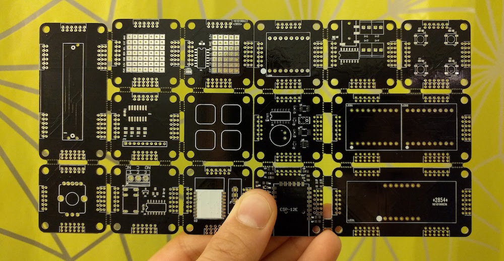
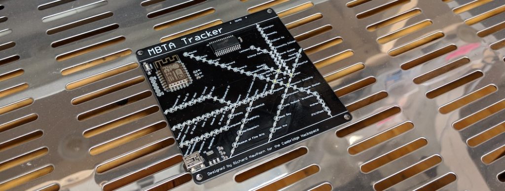
The history of Traintrackr can briefly be described as ‘tinkering with PCBs until I found something other people wanted to buy’. I designed around 100 PCBs before I came up with the first MBTA subway design, most of which were shown to people around me at the Cambridge Hackspace. It was a good way to improve my PCB designing skills, and a great way to receive feedback along the way. The MBTA PCB got people’s attention, you could see it in their faces once they realized what the blinking LEDs meant, and it was the start of Traintrackr.
Back at school in the late 90s we used a milling machine to fab our own single sided PCBs, it was a bit fiddly, but we managed to get some boards out of it. At the Cambridge Hackspace we had a CNC and the bits to mill PCBs, but despite a few attempts I never managed to successfully get up and running. Despite designing and manufacturing boards professionally over many years, I had never made one for fun. It was at this point that I learnt how easy manufacturing in China was, so decided to give it a go.
I started using Dirty PCBs, they offer good prices and all of my early boards were fabbed there. At the time you could get 10 x (50mm x 50mm) boards for $14 including delivery. Amazing considering that the densely populated boards I was designing would be basically impossible to make myself. Despite the name the quality was great, and they all worked perfectly.
Some companies only want to deal with single designs and charge extra if you want to panelize various boards into 1 mini panel, Dirty PCBs don’t mind and will happily fab anything you send them. This can be useful if, like me, you want to build 15 mini PCBs and combine them into 2 x (100mm x 100mm) boards.
When it came to the MBTA board I moved to JLC PCB, partly because they were cheaper, but also because they had recently started their assembly service.
We assembled the prototypes ourselves, using solder paste and a solder stencil, applying all the components by hand before putting it in the oven to bake. We had a few false starts where the circuit breaker tripped, once we sorted those issues out the boards came out really well.
However, there was way too much manual labor involved, so we moved on to the JLC assembly service.
We couldn’t quite believe the price of the assembly service at first, as they are significantly cheaper than any other assembly service, especially at low volume. The caveat here is that although they have 30k components to hand, that doesn’t cover some of the basics like USB connectors, the ESP8266 chip we use, or many other non standard components you might need. They also sell themselves as a prototype service, so although the quality has been mostly good, sometimes a few boards have come back with minor issues (a component the wrong way around, a scratched board etc), they also only do 30 boards at a time.
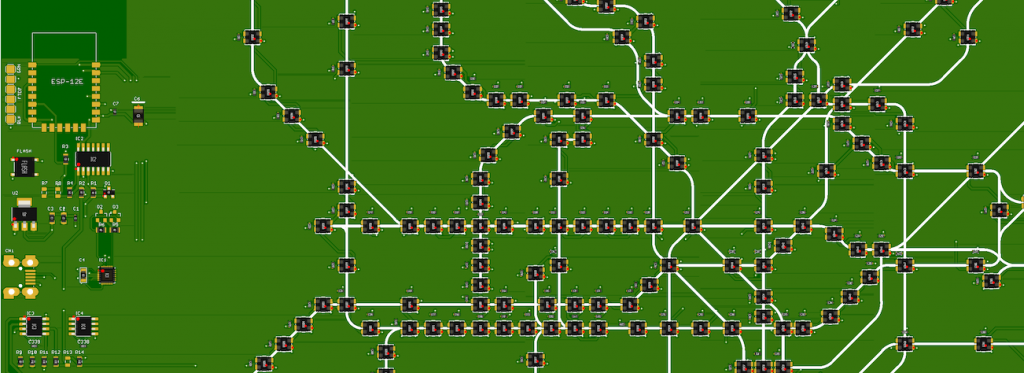
One big issue we found with them was on our Large London Underground product, we use 333 of the WS2812B-MINI LEDs on this design and each board had 2 or 3 failures which we had to fix manually. Some research showed that those LEDs are particularly sensitive to moisture when going through the reflow oven, and we assume JLC hadn’t been storing them appropriately.
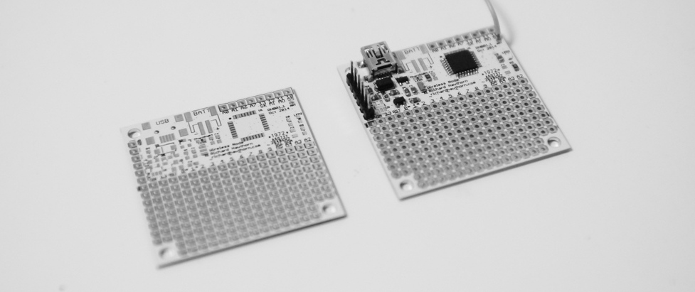
For our first MBTA board we used their prototype service, hand soldering the ESP8266 and USB connector ourselves. This worked well, and the price was almost the same as buying the boards, buying all the components, and assembling it all ourselves. Despite still having to assemble a couple of components ourselves, the price was truly amazing.
Getting your boards made
There are several stages in getting your data ready for assembly. You’ll need your GERBER file (showing the physical layout of the board), bill of materials (BOM), and your placement file, showing where on the board all the components go, including their orientation. These can all be exported from your PCB design software, although the BOM has to be adjusted quite a bit to fit into the template required by JLC. Once you get the hang of this it’s not too hard, but it took a while to work out what was needed.
There are 3 main parts of the placement file, the side of the board each part is going on (although JLC only assemble one side), the position of the component, and the orientation. It seems that each board house has their own ideas of what 90 degrees looks like, partly based on the orientation of the components as they come out of the tape, and partly based on the software you/they are using. It’s also confusing that the component orientation is calculated anti-clockwise, and not clockwise, which takes some getting used to.
With this in mind JLC will actually manually rotate everything based on the markings on the board, so make sure you have board markings, and make sure they are in the right place. JLC will often email you with an image to confirm the orientation once you have ordered, asking you to add markings in the future. Knowing these markings are right before you submit your order makes things a lot less stressful. One thing to note is that the markings on the board should match up with the makings on the component, which may not be pin 1. A standard IC will have pin 1 marked, but some components have a different pin marked (the WS2812-MINI has pin 3 marked). For these components make sure the marking on your silk screen matches up with the marking on the component.
JLC give you an assembly preview of the files you have uploaded, which is reassuring when you’re about to spend money on your first assembly job. It’s really helpful to make sure everything looks correct, the components are in the right place, and the orientation is correct (although they will fix this if they spot an issue)
After several orders from JLC the HT16K33 chips that we were using the drive our LEDs became harder to find, to the point where JLC removed them from their database. On our larger boards we had 5x of these chips, each with 28 pins. Where previously we were hand soldering 25 pins (for the ESP8266 and USB connector), we now had to add another 140, this wasn’t going to work for us.
At this point we were starting to build bigger products, and wanted them in larger volumes. JLC had been good at small scale (and was still perfect for prototyping), but we needed a larger manufacturer. We did some research and went to ALLPCB to manufacture our first batch of 100 MBTA dual direction boards.
The process here is very similar to JLC, although less automated. You supply them your gerber, BOM, and placement file, they quote you the assembly and the PCB costs upfront, but manually price the parts. This is usually back in a day or two. JLC have a huge catalogue of parts to hand (so they can quote your prices right away), ALLPCB have to order all the parts in, so need the time to do that.
I was a bit nervous about ordering 100 boards only to find they had put all the LEDs on back to front (any other component we could have fixed by hand if we really wanted, replacing 500 LEDs per board would not have been viable) but I didn’t need to worry. For every assembly order they will assemble the first board, confirming with you before they make the rest. This starts with photos of the board from a few angles, and gives you your first indication on how the assembly went.
We made the mistake in asking them to program the board so we could see it working. The instructions I sent didn’t make any sense to them, and I wasted a few days trying to explain before they suggested they send me the board to verify myself. Although this adds a bit of cost and time, it’s really reassuring to test the board yourself before the rest of the order is assembled. This is what we do for every production run, so we have a higher confidence that the batch is going to be successful.
We have recently built a board programmer which we will be sending to ALLPCB, which will let them flash firmware to each board, to verify that everything works. This means that any issues found can be corrected over there, saving us any rework when we receive them here. So as we move to higher volumes of boards from them, we can be confident that they are delivering boards that are ready to go, with minimal issues.